GL3525-S
USB 3.2 Gen1 Hub Controller with Power Delivery
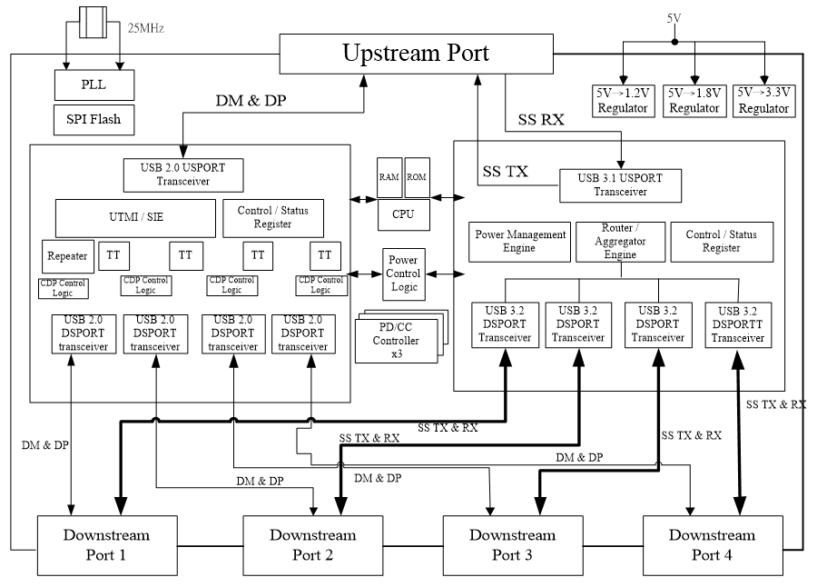
Genesys GL3525-S is a configurable USB3.2 Gen1 hub with power delivery controller. It is compliant with the USB 3.2 specification. GL3525-S integrates Genesys Logic self-developed USB 3.2 Gen 1 Super Speed transmitter/receiver physical layer (PHY) and USB 2.0 High-Speed PHY. It supports Super Speed, Hi-Speed, and Full-Speed USB connections and is fully backward compatible to all USB 2.0 and USB 1.1 hosts. GL3525-S also implements multiple TT* (Note1) architecture providing dedicated TT* to each downstream (DS) port, which guarantees Full-Speed (FS) data passing bandwidth when multiple FS devices perform heavy loading operations. Furthermore, GL3525-S has built-in 5V to 3.3V and 5V to 1.2V regulators, which saves customers’ BOM cost, and eases for PCB design.
GL3525-S features the native fast-charging and complies with USB-IF battery charging specification rev1.2, it could fast-charge Apple, Samsung Galaxy devices, and any device complaint with BC1.2/1.1. It also allows portable devices to draw up to 1.5A from GL3525-S charging downstream ports (CDP1) or dedicated charging port (DCP2). It can enable systems to fast charge handheld devices even during “Sleep” and “Power-off” modes.
GL3525-S features the native fast-charging and complies with USB-IF battery charging specification rev1.2, it could fast-charge Apple, Samsung Galaxy devices, and any device complaint with BC1.2/1.1. It also allows portable devices to draw up to 1.5A from GL3525-S charging downstream ports (CDP1) or dedicated charging port (DCP2). It can enable systems to fast charge handheld devices even during “Sleep” and “Power-off” modes.
And more, GL3525-S features advanced 3-Port PD controller that supports DisplayPort Alternate mode and charge-through function. It is compliant to USB Power Delivery Specification Rev3.0 /2.0 and Type-C Port Controller Specification R2.0. The GL3525-S integrates Type-C Channel Configuration (CC) function and BMC PHY to support PD messaging for power negotiation, power/data/Vconn swapping and Alternate mode function. The Type-C Port Manager (TCPM) for policy of 3 PD ports is achieved by I2C communication which is compliant with TCPCI R2.0 spec.
GL3525-S supports OVP/OCP/OTP with integrated 16-channel 10-bit ADC. There are threshold comparators for each ADC channel, so the protecting activity can be made very quickly once an over-or-under VBUS voltage, VBUS current, or temperature occurs.
In response to different applications, GL3525-S provides five port configurations with three packages, GL3525-OVAS1, GL3525-OVBS1 and GL3525-OVCS1.
GL3525-OVAS1 targets the dongle applications, has 3 VBUS charge pump pins and 2 sys5V charge pump pins for power path control. It also has VBUSDET pin to handle bleed discharge and integrates the SBU/AUX switch to support DisplayPort Alternate Mode on USB-C.
Both GL3525-OVBS1 and GL3525-OVCS1 target docking and monitor applications, and with firmware setting, both of parts can provide two different port configurations. The difference between GL3525-OVBS1 and GL3525-OVCS1 is that GL3525-OVCS1 provides two HPD pins to handle two DisplayPort sources or sinks while GL3525-OVBS1 only provides one HPD pin to handle one DisplayPort single.
GL3525-OVBS1 and GL3525-OVCS1 have 2 VBUS charge pump pins for power path control, and VBUSDET pin to handle bleed discharge or DISCHG pin to handle force discharge function. Both PD ports can be source, sink and DRP, which can be set according to the targeted application.
*Note: TT (transaction translator) implements the control logic defined in Section 11.14 ~ 11.22 of USB specification revision 2.0. TT basically handles the unbalanced traffic speed between the USPORT (operating in HS) and DSPORTS (operating in FS/LS) of hub.
---------------------------------------------
1 CDP, charging downstream port, the Battery Charging Rev.1.2-compliant USB port that does data communication and charges device up to 1.5A.
2 DCP, dedicated charging port, the Battery Charging Rev.1.2-compliant USB port that only charges devices up to 1.5A, similar to wall chargers.
1 CDP, charging downstream port, the Battery Charging Rev.1.2-compliant USB port that does data communication and charges device up to 1.5A.
2 DCP, dedicated charging port, the Battery Charging Rev.1.2-compliant USB port that only charges devices up to 1.5A, similar to wall chargers.
The available parts for GL3525-S are listed in the following table.
|
Part Number
|
Targeted Application
|
# of total ports
(UFP+DFP) |
# of native USB-C data ports
|
# of HPD
|
# of CC logic ports
|
GPIOs
|
|---|---|---|---|---|---|---|
|
GL3525-OVAS1
(QFN88) |
USB-C Dongle
|
2 USB-C SS +
2 USB-A SS + 1 HS |
2
|
1
|
3
|
1
|
|
GL3525-OVBS1
(QFN88) |
USB-C
Docking/ Monitor |
1 USB-C SS +
4 USB-A SS |
1 or 2
(depending on port configuration) |
1
|
3
|
1
|
|
2 USB-C SS +
2 USB-A SS + 1 HS |
||||||
|
GL3525-OVCS1
(QFN88) |
USB-C
Docking/ Monitor |
1 USB-C SS +
3 USB-A SS + 1 HS |
1
(depending on port configuration) |
2
|
3
|
6
|
|
5 USB-A SS
|
GL3525-S Package
The default configuration of GL3525-OVBS1 is 1 x USB-C SS port (Port W) + 4 x USB-A SS ports (Port X, Y, Z and V), and the Port X and Y can be combined as a USB-C port to make the configuration to be 2 x USB-C SS port (Port W and Port XY) + 2 x USB-A (Port Z and V) + 1 x HS port (from the original Port X).
The default configuration of GL3525-OVCS1 is 5 x USB-A SS ports (Port W, X, Y, Z and V), and the Port X and Y can be combined as a USB-C port to make the configuration to be 1 x USB-C SS port (Port XY) + 3 x USB-A (Port W, Z and V) + 1 x HS port (from the original Port X).
-
Compliant with USB 3.2 Gen 1 Specification
-
Upstream port supports SuperSpeed (SS), HighSpeed (HS) and FullSpeed (FS) traffic
-
Downstream ports support SS, HS, FS, and LowSpeed (LS) traffic
-
1 control pipe and 1 interrupt pipe
-
Backward compatible to USB specification Revision 2.0/1.1
-
-
Featuring fast-charging on all downstream ports and upstream port
-
Compliant with USB Battery Charging Revision v1.2, supporting CDP, DCP, and ACA-Dock
-
Downstream ports can be turned from a Standard Downstream Port (SDP) into Charging Downstream Port (CDP) or Dedicated Charging Port (DCP)
-
Downstream devices can be charged while upstream VBUS is not present, which can be applied on wall charger applications
-
Upstream port is capable of charging and data communicating simultaneously for portable devices supporting ACA-Dock or proprietary charging protocols
-
Supporting Apple 1A/2.1A/2.4A and Samsung Galaxy devices fast-charging
-
- Firmware recovery supported
-
256Kbyte for dual regions of firmware
-
-
Multiple Transaction Translator (TT) architecture
-
Providing dedicated TT control logics for each downstream port
-
Superior performance when multiple FS devices operate concurrently
-
-
Integrated USB transceiver
-
Improving output drivers with slew-rate control for EMI reduction
-
Internal power-fail detection for ESD recovery
-
-
Advanced power management and low power consumption
-
Supporting USB 3.2 U0/U1/U2/U3 power management states
-
Supporting USB Link Power Management (LPM) L0/L1/L2
-
Supporting individual/gang mode over-current detection for all downstream ports
-
Supporting both low/high-enabled power switches
-
Patented Smart Power Management
-
-
Configurable settings by firmware
- Configurable charging port
- Configurable SuperSpeed and HighSpeed downstream ports, downstream port can be disabled/enabled by each specific port for USB3.2/USB2.0
- Supporting full in-system programming firmware upgrade
- Supporting compound-device (non-removable setting on downstream ports)
- Supporting customized VID/PID
-
Power Delivery features
-
USB Power Delivery Spec 3.0 /2.0 compliant
-
Compliant to Type-C port controller specification (TCPCI) R2.0
-
Support high voltage protection for CC to prevent short-to-VBUS
-
Support Device Policy Manager and Type-C Port Manager (TCPM)
-
Support 3PD ports with charge-through function and DisplayPort Alternate mode on Type-C
-
Support all Type-C Channel Configuration (CC) function and BMC PHY.
-
Support configurable Source, Sink and DRP (Source-Sink)
-
Support configurable Dead Battery function by different package
-
Support built-In 5V VCONN power switch
-
Support built-In 16-channel 10bit ADC to monitor VBUS voltage, VBUS bi-directional current, temperature
-
Support SBU/AUX switch for DisplayPort Alternate mode function with high voltage protection
-
Support power selection to select the highest voltage among VBUSDET1~3 and sys5V as HVLDO’s power source
-
3 VBUS charge pump pins and 2 sys5V charge pump pins flexibly control power switch on power path
-
-
Flexible design
-
Supporting Poly-fuse/Power-switch
-
Automatic switching between self-powered and bus-powered modes
-
Supporting electrical tuning for each specific port
-
GPIOs can be programmed as I2C interface to access other controllers
-
-
Low BOM cost
-
Single external 25 MHz crystal / Oscillator clock input
-
Built-in upstream port 1.5KΩ pull-up and downstream port 15KΩ pull-down resistors
-
Built-in 5-to-3.3V, 5-to-1.2V and 5-to-1.8V regulator
-
-
Miscellaneous
-
Hotkey detection on the single assigned port
-
Billboard/USB-C bridge integrated
-
HID integrated
-
-
Applications
-
USB-C Video Adapters with PD Charging through dongles
-
USB-C Multi-function Dock
-
USB-C Monitor
-
USB/PD wall charger
-
Other consumer electronics
-
GL3525-S