GL3004
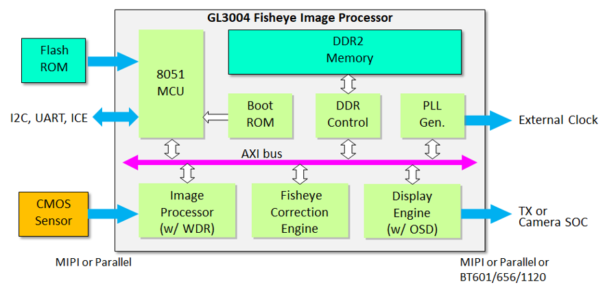
The GL3004 integrates fisheye correction engine, image processor, display engine, MCU 8051, memory controller and common interface, including 2-lane MIPI (TX/RX), DVP (in/out) and BT601/656/1120 output interfaces. The SPI flash and DDR2 memory are also embedded in the GL3004 MCP package in order to reduce product PCBA area.
GL3004 is a dedicated fisheye image processor for wide-angle application. The proprietary dewarping engine provides various mathods of fisheye correction. The complete image signal processing (ISP) offers true color processing capabilities.The display engine accomplishs a rich dewarping effect that satisfies the diversity of wide-angle scenes and enhances human visual experience. The detail features of the GL3004 are described below:
1.1 Fisheye Correction Modes
- Customized Fisheye Correction
- Spherical Panorama Dewarping
- Perspective Projection Dewarping
- Three views Stitching
- Panorama View
- Single View
- Bird View
- Corner Views
- Multi-Views
- 360°and ePTZ
- Mirror/Flip
- 4-Layer Graphic OSD
- Dynamic Overlay
- Font OSD
- Bad Pixel Correction
- Gr/Gb Green Balance
- Black Level Compensation
- Lens Shading Correction
- Denoise
- Edge Enhancement
- Bayer Patten Interpolation (Color Interpolation)
- Auto-White-Balance
- Auto-Exposure
- Color Correction Matrix
- Gamma
- YUV Processing (for brightness, contrast, hue, gain, and offset processing)
- Wide Dynamic Range (WDR)
- Input interface: 2-lane MIPI or 12-bit parallel
- Output interface: 2-lane MIPI or 12-bit parallel or BT601/656/1120
- Input resolution up to 3M @30fps
- Input data format:
- 8/10/12-bit Bayer RAW
- Output resolution up to 2M @30fps or 3M @20fps
- Output data format:
- 8/10/12-bit Bayer RAW
- 8/16-bit YUV 4:2:2
- Cyclone-8051 is an improved and compatible with the legacy 8-bit 80C51/52 CPU
- A 4-stage pipeline architecture that enables to execute most of the instructions in a single clock cycle
- Speed is on average 9 times faster than the legacy 80C51/52
- Reference Clock: 24MHz
- Clock Output 1: 1056MHz ~ 384MHz. Step : 48MHz
- Clock Output 2 = Clock Ouptut 1 divided by 2
- SSC (Spread Spectrum Clocking) function
- Reference Clock: 24MHz
- VCO Clock: 384MHz ~ 499.2MHz. Step : 4.8MHz
- Clock Output 1 = VCO Clock divided by 2 ~ 4
- Clock Output 2 = VCO Clock divided by 5 ~ 9
- SSC (Spread Spectrum Clocking) function
- DDR2 mode & signaling; rates from 100Mbps up to 800Mbps
- 1.8V/1.5/1.2V SSTL JEDEC standard
- Multiple drive strengths adjustable
- Independent read and write timing adjustments with auto calibration
- Per bit de-skew support
- PVT compensation and timing calibration for all corner reliability
- Mixed-signal D-PHY mixed-signal hard-macro-HS/LS Transmitter and LS/HS Receiver solution
- Designed to MIPI® v1.0 Specifications
- 1.0GHz maximum data transfer rate per lane
- Expandable to support 2 data lanes, providing up to 2Gbps transfer rate
- HS, LP and ULPS modes supported
- 10Mbps per lane in low-power mode
- Unidirectional and bi-directional modes supported
- Automatic termination control for HS and LP modes
- Low-Power dissipation: less than 3mA/Lane in HS TX/RX mode
- Tx/Rx Buffers with tunable On-Die-Termination and advanced equalization
- Embedded ESD, boundary scan support logic
- SPI Master, TWI Bus interfaces
- UART, GPIOs
- Power Supplies: 1.2V ±10%, 1.8V ±10%, 3.3V ±10%
- Typical power consumption: < 600mW for DVP @input 1080P30, output 720P30
- QFN76 MCP (Multi Chip Package) with 128Mbit DDR2 DRAM and 2Mbit SPI Flash dies
- Industrial Grade: -40°C to 85°C